日本电子制造商东芝公司推出了一种基于碳化硅(SiC)的新型金属氧化物半导体场效应晶体管(MOSFET),主要应用于太阳能逆变器和电池存储系统。
该公司表示,新的MOSFET可能有助于逆变器制造商减小其产品的尺寸及重量。
该公司还提到:“高频运行可以减少其他系统组件的体积和重量,如散热器和过滤器等。”
新产品包含一个2200 V肖特基势垒二极管(SBD),主要应用于1500 V(直流电)两电平逆变器。据制造商介绍,两电平设备相比三电平逆变器,具有更少的开关模块,因此系统体积更小、质量更轻。
据报道,SiC模块具有低传导损耗和低漏源电压的特点。它们导通和关断的开关损耗也较低,分别为14mJ和11mJ。据称,它们具备低漏感、低热阻特性并内置了热敏电阻。
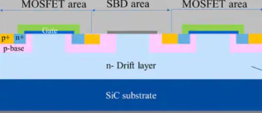
东芝2200 V SiC MOSFET横截面示意图
图片来源:东芝集团
This content is protected by copyright and may not be reused. If you want to cooperate with us and would like to reuse some of our content, please contact: editors@pv-magazine.com.











By submitting this form you agree to pv magazine using your data for the purposes of publishing your comment.
Your personal data will only be disclosed or otherwise transmitted to third parties for the purposes of spam filtering or if this is necessary for technical maintenance of the website. Any other transfer to third parties will not take place unless this is justified on the basis of applicable data protection regulations or if pv magazine is legally obliged to do so.
You may revoke this consent at any time with effect for the future, in which case your personal data will be deleted immediately. Otherwise, your data will be deleted if pv magazine has processed your request or the purpose of data storage is fulfilled.
Further information on data privacy can be found in our Data Protection Policy.